Materialien
III-V-Photonik-Epitaxie-Wafer
Deliver high-performance lasers, detectors, and other III-V semiconductor optoelectronic devices by fabricating with our consistent, high-quality epitaxial wafers.
The Coherent foundry employs a state-of-the-art MOCVD platform to deliver wafers which set a new standard for quality, performance, and yield. These meet the demands of challenging industrial, automotive, military, and communications applications.
III-V Photonics Wafer Capability
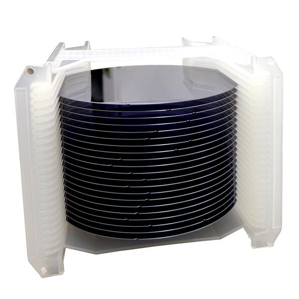
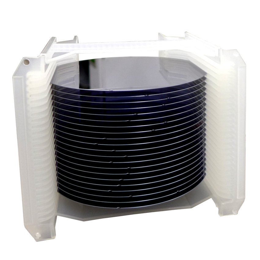
Source 2-inch to 6-inch wafers fabricated in our 25,000 square foot, Class 1000 cleanroom facility.
Device Type |
Base Material |
Material Capability |
Wafer Diameter |
EpiLaser® (VCSEL, EEL, LED) |
GaAs |
AlGaAs/GaAs, InGaP/GaAs, InAlGaP |
up to 150mm |
InP |
InP/InGaAs, InGaAsP, InAlAs, InAlGaAs |
up to 100mm |
|
EpiDetector® (P-i-N, APD) |
GaAs |
AlGaAs/GaAs, InGaP/GaAs |
up to 150mm |
InP |
InP/InGaAs, InGaAsP, InAlGaAs |
up to 100mm |
|
EpiSolar™ (1J, 2J, 3J, 4J) |
GaAs, Ge |
InGaP/GaAs/InGaAs, InAlGaP, AlGaAs |
up to 150mm |
InP |
InP/InGaAs, InGaAsP, InAlAs, InAlGaAs |
up to 100mm |
Verwandte Produkte
Empfohlener Blog
SiC Circuitry Makes EVs Better
Coherent is one of the few companies worldwide with a complete, vertically integrated SiC manufacturing capability. We produce SiC wafers and epitaxy, all the way through power devices and modules. Furthermore, the unmatched quality with which we can produce SiC material makes Coherent virtually the only supplier positioned to successfully transition from the current standard wafer diameter of 150 mm up to 200 mm.

Ausgewählte Erfolgsgeschichte
Laser Framework setzt neue Maßstäbe in der Digital Factory von Siemens
Dank der Unterstützung bei der Coherent und der Coherent FrameWork“-Software kann Siemens sein ID-Link-Fertigungsprogramm erfolgreich umsetzen.
